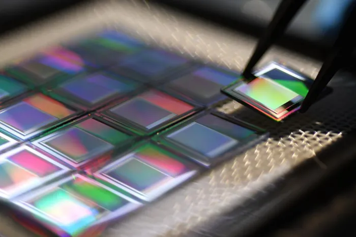
A microbolometer is one of the most important components in an uncooled infrared camera. It detects infrared radiation by converting the heat absorbed from the scene into a change in electrical resistance. An array of thousands or even millions of microbolometer pixels can then be used to create a thermal image.
Unlike cooled infrared detectors, microbolometers do not require a cryogenic cooling system. This makes them smaller, lighter, lower in power consumption, and easier to integrate into thermal cameras.
But how does a microbolometer actually work? What is a microbolometer made of, and why are parameters such as pixel size and NETD important? This article explains the basics in simple terms.
What is a Microbolometer?
A microbolometer is a miniature thermal detector designed to detect infrared radiation. The word comes from two parts: “micro,” referring to its very small size, and “bolometer,” a device that measures radiation through changes in temperature and electrical resistance.
A typical microbolometer contains a large number of tiny sensing elements arranged in a two-dimensional array. Each element acts like a small temperature-sensitive resistor. When infrared radiation reaches a pixel, the absorbing material heats up slightly. This temperature change causes its electrical resistance to change. The readout circuit then measures this change and converts it into an electrical signal.
When this process takes place across the entire array, the camera obtains a two-dimensional map of infrared radiation. Image-processing electronics can then convert the signals into a visible thermal image.
For example, a 640×512 infrared detector contains 327,680 pixels. Each pixel collects information from a small area of the scene. Together, these pixels form the thermal image.
This is why a microbolometer should not simply be understood as a “tiny thermometer.” It is better described as a pixel-level infrared detector that responds to changes in absorbed thermal radiation.
How Does a Microbolometer Work?
The working principle of a microbolometer is relatively simple.
Every object above absolute zero emits electromagnetic radiation. At ordinary environmental temperatures, much of the emitted thermal radiation falls within the infrared region. A thermal camera uses an infrared lens to focus this radiation onto the detector array.
When the radiation reaches a microbolometer pixel, an absorber captures part of the infrared energy. The absorbed energy causes the sensing element to warm slightly. Because the sensing material has a temperature-dependent electrical resistance, its resistance changes as its temperature changes.
The change is very small, so the detector must be carefully designed to make the signal measurable. A readout integrated circuit, or ROIC, is placed beneath the detector array to measure and process the electrical signal from individual pixels.
The basic signal chain can therefore be understood as:
Infrared radiation → absorption → temperature change → resistance change → electrical signal → image processing → thermal image
The microbolometer itself does not directly produce the final color thermal image seen on a display. The detector generates electrical signals, while the ROIC, calibration system, and image-processing algorithms turn those signals into usable thermal data.
This distinction is important when evaluating an infrared camera. Image quality does not depend on the detector alone. The optics, detector, readout circuit, calibration, image processing, and other system components all contribute to the final result.
What is a Microbolometer Made of?
Modern microbolometers are usually built as microstructures using MEMS-based semiconductor manufacturing processes. A typical pixel includes an infrared absorber, a temperature-sensitive material, supporting structures, and a cavity that provides thermal isolation from the substrate.
Thermal isolation is particularly important. If heat from the absorbing element quickly flows into the substrate, the temperature change caused by infrared radiation will be very small and difficult to measure. A suspended microbridge structure helps reduce this heat loss and allows the pixel to respond more effectively to incoming radiation.
Two materials commonly used in uncooled microbolometers are vanadium oxide (VOx) and amorphous silicon (a-Si). Both have temperature-dependent electrical properties that make them suitable for infrared detection.
The detector is usually fabricated together with or integrated closely with a CMOS readout circuit. This semiconductor-based manufacturing approach is one of the reasons microbolometer arrays can be produced in large quantities and integrated into compact infrared modules.
Why are Microbolometers Usually Uncooled?
One of the biggest advantages of a microbolometer is that it can operate at or near room temperature.
Some high-performance infrared detectors, particularly quantum detectors used in cooled infrared cameras, require cooling to very low temperatures. Cooling improves sensitivity and response speed, but it also adds a cooler, power consumption, mechanical complexity, size, and cost to the system.
Microbolometers use a different detection principle. They detect the heating effect of infrared radiation rather than relying on direct photon detection. Therefore, they do not normally need cryogenic cooling.
This makes uncooled microbolometers especially attractive when the system needs to be compact, reliable, power-efficient, and cost-effective.
The trade-off is that cooled infrared detectors can generally provide higher sensitivity and faster response, particularly for demanding applications. A microbolometer is therefore not automatically “better” than a cooled detector. The right technology depends on the application, performance target, size, power, and cost requirements.
What Are the Key Microbolometer Performance Parameters?
Several specifications are important when selecting a microbolometer detector. Among them, NETD, pixel pitch, resolution, spectral response, and frame rate are particularly important.
NETD
NETD stands for Noise Equivalent Temperature Difference. It is one of the most commonly used indicators of thermal sensitivity.
In simple terms, NETD describes the smallest temperature difference that an infrared imaging system can distinguish under specified test conditions. A lower NETD generally indicates better sensitivity. For example, a detector with a NETD of 30mK is generally more sensitive to small temperature differences than one with a NETD of 50mK, assuming the measurement conditions are comparable.
However, NETD should not be viewed in isolation. The actual image performance also depends on the lens, f-number, integration time, signal processing, calibration, and test conditions.
Modern uncooled microbolometer systems can achieve NETD values in the range of a few tens of millikelvin. For example, commercial 12μm uncooled microbolometer systems are available with NETD specifications around 30–50mK.
Pixel Pitch
Pixel pitch is the distance from the center of one detector pixel to the center of the next. It is commonly expressed in micrometers (μm).
Smaller pixel pitch allows more pixels to be placed within the same detector area. This can help manufacturers achieve higher resolution or make the detector smaller for a given resolution.
The development of microbolometers shows a clear trend toward smaller pixel sizes. Research literature reports a reduction from about 50μm in early microbolometer development to 25μm, 17μm, and 12μm, with advanced technologies reaching around 10μm.
However, smaller does not automatically mean better. Reducing pixel size also reduces the area available to collect infrared radiation. Maintaining sensitivity while shrinking the pixel therefore requires improvements in the detector structure, thermal isolation, materials, readout electronics, and manufacturing process.
Resolution
Resolution describes the number of pixels in the detector array. Common formats include 384×288, and 640×512, while higher-resolution arrays such as 1280×1024 are also available. For example, a 640×512 array contains more than 327,000 individual pixels, while a 1280×1024 array contains more than 1.3 million pixels.
Higher resolution can provide more image detail, but it may also increase data volume, processing requirements, and system cost. The best resolution depends on the required detection distance, field of view, lens selection, and application.
Spectral Response
A microbolometer can be designed to respond to a specific infrared wavelength range.
Many uncooled thermal cameras operate in the long-wave infrared (LWIR) band, commonly around 8–14μm. This range is particularly useful for imaging objects near ambient temperature and is widely used in industrial inspection, building diagnostics, security monitoring, and other thermal imaging applications.
The spectral response should therefore be selected according to the target and application. A detector designed for LWIR thermal imaging is not necessarily suitable for every infrared sensing task.
Frame Rate and Thermal Time Constant
Frame rate describes how many images the system can capture each second. Higher frame rates are useful when the target or camera is moving quickly.
Another related parameter is the thermal time constant. It describes how quickly the detector responds to a change in infrared radiation. A shorter thermal time constant generally means a faster detector response. Research on uncooled infrared detectors has shown that thermal time constant and sensitivity are closely related to the design of the detector's suspended structure.
In practice, detector sensitivity and response speed must be balanced. Improving one parameter may affect another, so microbolometer design is always a system-level optimization.
Microbolometer vs. Cooled Infrared Detector
The biggest difference between a microbolometer and a cooled infrared detector is the detection and operating method.
A microbolometer is normally an uncooled thermal detector. It detects infrared radiation through the temperature-induced resistance change of its sensing element. It does not require a cryogenic cooler and is therefore well suited to compact and cost-sensitive thermal imaging systems.
A cooled infrared detector, by contrast, often uses a quantum detection material such as InSb or HgCdTe and operates with a cryogenic cooler. The cooling system reduces detector noise and enables very high sensitivity and fast response. However, it also makes the camera more complex, larger, and more power-hungry.
For this reason, microbolometers are widely used when compact size, low power consumption, reliability, and cost are important. Cooled detectors are more often selected when extremely high sensitivity, long-range imaging, high-speed measurement, or other demanding performance requirements justify the additional system complexity.
The choice is therefore not simply between “good” and “better.” It is a matter of matching detector technology to the application.
Conclusion: Microbolometers Are at the Heart of Uncooled Thermal Imaging
A microbolometer is a miniature infrared detector that converts absorbed infrared radiation into an electrical signal through a temperature-dependent resistance change. When thousands or millions of these pixels are arranged into a focal plane array, they form the sensing core of an uncooled thermal camera.
Its biggest advantage is the ability to provide practical infrared imaging without a cryogenic cooling system. This enables compact, low-power, reliable, and relatively cost-effective thermal imaging systems.
As pixel pitch continues to decrease and detector materials, MEMS structures, ROICs, packaging, and image-processing technologies continue to improve, microbolometers are becoming more capable while remaining suitable for compact infrared systems.
For anyone working with thermal cameras, infrared modules, or uncooled infrared detectors, understanding the microbolometer is therefore a useful starting point. It is the small sensing element that turns invisible infrared radiation into the thermal images we can see and analyze.


 CN
CN
 EN
EN