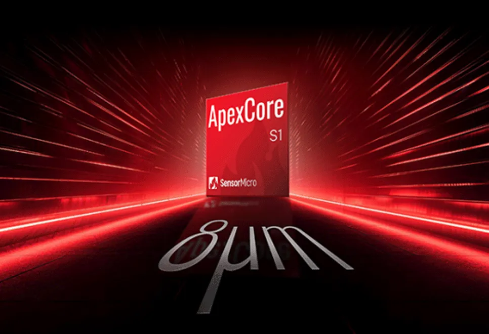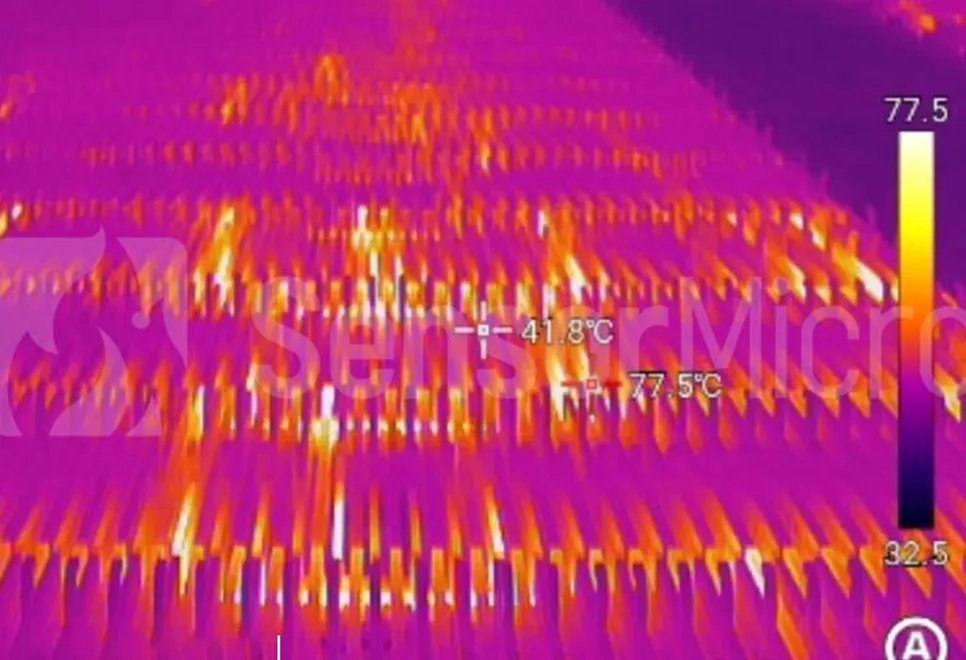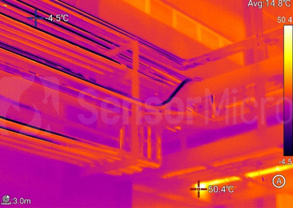
As infrared thermal imaging technology continues to advance, infrared detectors and camera cores are becoming increasingly intelligent and compact. Behind every high-performance infrared imaging system, powerful processing chips play a critical role in converting raw infrared signals into clear images and accurate temperature data. When exploring infrared detectors, thermal camera cores, and imaging modules, users often encounter terms such as FPGA, ASIC, SoC, and MCU. These technologies represent different types of processing architectures that handle image processing, algorithm execution, data conversion, and system control. Among them, FPGA and ASIC are two of the most widely used processing solutions in infrared thermal imaging systems. Although both are designed to process digital signals and improve imaging performance, they differ significantly in flexibility, cost, power consumption, size, and application scenarios.
What is FPGA in Infrared Thermal Imaging?
FPGA (Field Programmable Gate Array) is a programmable semiconductor device with a reconfigurable hardware architecture. Unlike traditional processors, FPGA allows users to modify internal logic units and connections through programming, enabling customized processing functions after manufacturing. In infrared imaging systems, FPGA is commonly used for tasks such as infrared image enhancement, non-uniformity correction (NUC) , image filtering and noise reduction, video processing, and data communication control.
The biggest advantage of FPGA is its flexibility. Engineers can modify algorithms and update hardware logic according to different application requirements, making it suitable for projects that require frequent upgrades or rapid development cycles.
What is ASIC in Infrared Thermal Imaging?
ASIC (Application Specific Integrated Circuit) is a customized integrated circuit designed for a specific application or function. Unlike FPGA, which provides programmable flexibility, ASIC is developed with a fixed hardware architecture optimized for a particular algorithm or system requirement. Once designed and manufactured, its functions cannot be changed. In infrared thermal imaging applications, ASIC chips are often used for dedicated image processing tasks, including infrared signal processing, image correction algorithms, temperature calculation, low-power image processing, and high-speed data processing. Because ASIC is specifically optimized for a target application, it can achieve higher efficiency, smaller size, and lower power consumption compared with general programmable solutions.
FPGA vs. ASIC: Development and Flexibility
One of the biggest differences between FPGA and ASIC is the development approach. FPGA requires engineers to configure and modify internal logic through programming. This process provides significant flexibility because developers can update algorithms, add functions, or optimize performance even after deployment. ASIC, on the other hand, is designed for a specific purpose. Its circuit structure is fixed during manufacturing, meaning changes require a new chip design and production process. Therefore, FPGA offers higher flexibility and faster development cycles. ASIC provides optimized performance for mature and stable applications.
For infrared products that are still undergoing algorithm development or require frequent upgrades, FPGA is often the preferred choice. For products with mature functions and large-scale production requirements, ASIC provides better long-term advantages.
FPGA vs. ASIC: Cost Comparison
Cost is another important factor when selecting an infrared processing chip.
FPGA devices contain programmable logic resources and additional hardware structures, which increase manufacturing costs. However, they do not require expensive custom chip development, making them suitable for small and medium production volumes. ASIC requires significant investment in chip design, verification, and manufacturing preparation. The initial development cost is usually higher than FPGA.
However, once production volume increases, ASIC has a major cost advantage. Because it is optimized for a specific function and requires fewer unnecessary components, the cost per chip can become significantly lower than FPGA. This makes ASIC particularly suitable for high-volume commercial products.
FPGA vs. ASIC: Size and Power Consumption
For modern infrared thermal imaging systems, size, weight, and power consumption (SWaP) are increasingly important, especially in applications such as drones, unmanned systems, handheld devices, and aerospace platforms. In terms of size, ASIC usually has an advantage because the circuit is highly integrated and optimized for a specific function. Under the same processing requirements, an ASIC-based solution can achieve a smaller form factor.
Power consumption is another area where ASIC performs better. FPGA requires programmable logic resources to maintain flexibility, which generally results in higher energy consumption. ASIC eliminates unnecessary hardware structures and performs dedicated calculations more efficiently. Therefore, ASIC is often preferred for compact, low-power infrared camera cores and embedded thermal imaging systems.
The Role of Processing Chips in Future Infrared Thermal Imaging
As infrared thermal imaging continues to expand into industrial inspection, autonomous driving, medical imaging, security monitoring, aerospace, and smart devices, processing chips are becoming increasingly important.
Future infrared systems require higher resolution, faster processing speeds, lower power consumption, and stronger artificial intelligence capabilities. This trend is driving the development of more integrated solutions, including ASIC, SoC, and AI-based processing architectures.
Conclusion
FPGA and ASIC are two important processing technologies supporting modern infrared thermal imaging systems. FPGA provides excellent flexibility, rapid development capability, and algorithm adaptability, making it ideal for applications that require frequent updates or customized functions. ASIC delivers higher efficiency, lower power consumption, smaller size, and better cost performance for mature, large-scale products. There is no absolute winner between FPGA and ASIC. The right choice depends on the product stage, application requirements, production volume, and performance goals.
As infrared technology moves toward higher integration and smarter processing, the combination of advanced infrared detectors with optimized processing chips will continue to drive innovation in thermal imaging systems across industrial, commercial, and emerging applications.


 CN
CN
 EN
EN